- 6,6 MS/s mit Musterbreite von 8 Bit
- Ausgang für zusätzlichen Bezugstaktgeber
- Basierend auf VX Instruments FlexCPP für ein benutzerfreundliches Design
- Bis zu 2 unabhängige Module mit 4 gleichzeitig arbeitenden Kanälen
- Weitreichend konfigurierbare Trigger-Engine
- Mehrere Möglichkeiten zur Synchronisierung von Geräten und Kanälen
- Großer Bereich an Abtastraten aufgrund programmierbarer interner PLL
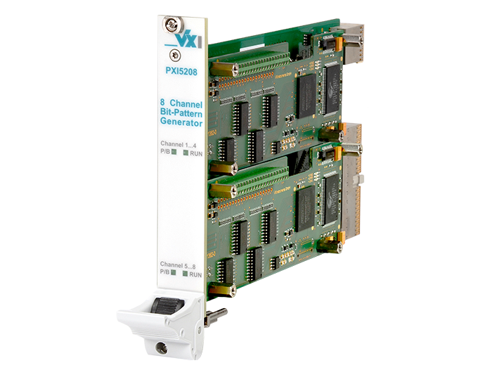
Die digitale I/O-Karte PXI(e)520x ist immer dann von Vorteil, wenn für die Signalausgabe oder Erfassung keine standardisierten Spannungs- oder Strompegel verwendet werden können. Mit dem digitalen Interface lässt sich eine vordefinierte Abfolge von Bit-Sequenzen ausgeben oder mit dem Receiver-Modul aufnehmen. Je nach Applikation können individuelle Ausgangsmodule entwickelt werden, um die geforderten Signalpegel zu realisieren.
Die Anschlussstecker sind ebenfalls frei definierbar.
|
Bestelloption
|
Kommentar
|
|
PXI5204
|
4 channel Bit-Pattern Generator
|
|
PXI5208
|
8 channel Bit-Pattern Generator
|